Welcome to Shenzhen Chengchi Circuit Technology Co., Ltd official website

CN Shenzhen Chengchi Circuit Technology Co., Ltd.
Service Hotline

+8618129931046 Mr. Liao

Shenzhen Chengchi Circuit Technology Co., Ltd.
EN
Shenzhen Chengchi Circuit Technology Co., Ltd. Shenzhen Chengchi Circuit Technology Co., Ltd.

News

Home >  News > 

Repeater PCB for Enhanced Signal Amplification and Transmission

Repeater PCB for Enhanced Signal Amplification and Transmission

Repeater PCB for Enhanced Signal Amplification and TransmissionFeb 21, 2025 Repeater PCB for Enhanced Signal Amplification and Transmission1

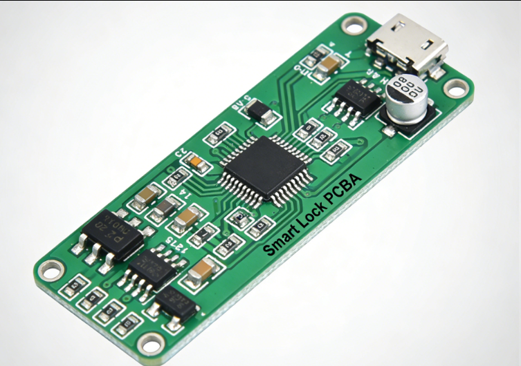
With the continuous development of science and technology, PCB board industry is also moving forward, technology upgrading has become a key element of the development of the industry...

Know MoreShenzhen Chengchi Circuit Technology Co., Ltd.

Clock Signal Optimization Design for Multilayer PCBs

Clock Signal Optimization Design for Multilayer PCBs

    Clock signal optimization is a critical aspect of designing multilayer printed circuit boards (PCBs), especially in high-speed digital systems. Proper clock signal design ensures reliable timing, reduces jitter, and minimizes electromagnetic interference (EMI).  One of the key considerations in

Clock Signal Optimization Design for Multilayer PCBsJun 26, 2025 Clock Signal Optimization Design for Multilayer PCBs1

DetailClock Signal Optimization Design for Multilayer PCBs

Applications of Multilayer PCBs in Industrial Automation Equipment

Applications of Multilayer PCBs in Industrial Automation Equipment

    Multilayer PCBs play a critical role in the design and functionality of industrial automation equipment. These boards are composed of multiple layers of conductive material separated by insulating layers, allowing for complex circuit designs and increased component density.  One of the primary a

Applications of Multilayer PCBs in Industrial Automation EquipmentJun 25, 2025 Applications of Multilayer PCBs in Industrial Automation Equipment1

DetailApplications of Multilayer PCBs in Industrial Automation Equipment

ENIG (Electroless Nickel Immersion Gold) Process for Multilayer PCBs

ENIG (Electroless Nickel Immersion Gold) Process for Multilayer PCBs

    ENIG, or Electroless Nickel Immersion Gold, is a popular surface finish for multilayer printed circuit boards (PCBs). This process is favored for its excellent surface planarity, good solderability, and wire bondability. The ENIG process involves depositing a layer of nickel followed by a thin l

ENIG (Electroless Nickel Immersion Gold) Process for Multilayer PCBsJun 25, 2025 ENIG (Electroless Nickel Immersion Gold) Process for Multilayer PCBs1

DetailENIG (Electroless Nickel Immersion Gold) Process for Multilayer PCBs

Design of Digital-Analog Mixed Circuits in PCB

Design of Digital-Analog Mixed Circuits in PCB

    The design of digital-analog mixed circuits in printed circuit boards (PCBs) presents unique challenges and requires careful consideration of various factors to ensure optimal performance. Digital circuits operate on discrete voltage levels representing binary values, while analog circuits deal

Design of Digital-Analog Mixed Circuits in PCBJun 24, 2025 Design of Digital-Analog Mixed Circuits in PCB1

DetailDesign of Digital-Analog Mixed Circuits in PCB

Application of Multilayer Boards in Smart Grid Equipment

Application of Multilayer Boards in Smart Grid Equipment

    Multilayer printed circuit boards (PCBs) play a crucial role in the development and operation of smart grid equipment, enabling the efficient management and distribution of electrical power. The smart grid, characterized by its integration of advanced information and communication technologies w

Application of Multilayer Boards in Smart Grid EquipmentJun 24, 2025 Application of Multilayer Boards in Smart Grid Equipment1

DetailApplication of Multilayer Boards in Smart Grid Equipment

Environmentally Friendly Surface Treatment Processes for PCB Boards

Environmentally Friendly Surface Treatment Processes for PCB Boards

    In an era of increasing environmental awareness and strict regulations, the development of environmentally friendly surface treatment processes for PCB boards has become imperative. Traditional surface treatment methods often involve the use of hazardous substances, such as lead-based solders an

Environmentally Friendly Surface Treatment Processes for PCB BoardsJun 24, 2025 Environmentally Friendly Surface Treatment Processes for PCB Boards1

DetailEnvironmentally Friendly Surface Treatment Processes for PCB Boards
  • <
  • 9
  • 10
  • 11
  • 12
  • 13
  • 14
  • 15
  • 16
  • 17
  • >
  • Save Time

    Save Time

    Save Money

    Save Money

    Save Labour

    Save Labour

    Free From Worry

    Free From Worry