-
CN
-
Service Hotline
+8618129931046 Mr. Liao


Time:2025-08-19 Views:1

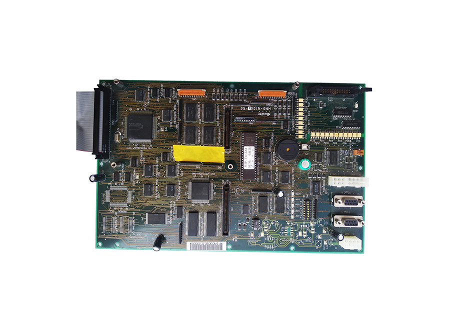
Ultra-High-Frequency (UHF) PCBs are specialized printed circuit boards designed to operate at frequencies above 300 MHz, with common applications spanning 5G communication modules, satellite transceivers, radar systems, and RF (radio frequency) sensors. Unlike standard PCBs (optimized for low-frequency digital or analog signals), UHF PCBs must address unique challenges related to signal integrity—specifically, minimizing signal loss, electromagnetic interference (EMI), and parasitic effects (inductance and capacitance) that degrade performance at high frequencies. These PCBs are critical in modern wireless technologies, where reliable transmission of high-speed data (up to several Gbps) over long distances or in complex environments is essential.
The foundation of UHF PCB performance lies in material selection, which directly impacts signal propagation. Traditional FR-4 epoxy glass substrates are unsuitable for UHF applications due to their high dielectric loss (Df, typically 0.02-0.04 at 1 GHz), which causes significant signal attenuation. Instead, UHF PCBs use low-loss materials such as PTFE (Polytetrafluoroethylene, e.g., Rogers 4350B), ceramic-filled composites (e.g., Rogers 6006), or liquid crystal polymers (LCP). These materials offer ultra-low dielectric loss (Df < 0.005 at 10 GHz for PTFE) and stable dielectric constant (Dk, typically 2.2-3.0) across temperature ranges (-40°C to 125°C), ensuring consistent signal speed and minimal loss. For example, a 5G base station’s UHF PCB uses Rogers 4350B substrate to transmit 28 GHz mmWave signals with <0.1 dB/inch attenuation, enabling reliable coverage over 500+ meters.
UHF PCB design also prioritizes controlled impedance to prevent signal reflections. Impedance (typically 50Ω or 75Ω for RF applications) is determined by the trace width, substrate thickness, and dielectric constant. Advanced design tools (e.g., ANSYS HFSS, Altium Designer) simulate signal paths to optimize trace geometry—for instance, a 50Ω microstrip trace on a 0.25mm thick PTFE substrate requires a 0.3mm width to maintain impedance. Additionally, UHF PCBs use ground planes (solid copper layers beneath signal traces) to reduce EMI and provide a low-resistance return path. For differential signals (common in UHF transceivers), paired traces with equal spacing from the ground plane minimize crosstalk (signal leakage between adjacent traces), which can distort high-frequency signals.
Manufacturing UHF PCBs requires precision processes to avoid material damage and maintain dimensional accuracy. PTFE substrates are difficult to drill due to their softness, so manufacturers use diamond-coated drills and controlled feed rates (50-100 mm/min) to create via holes with minimal burring. Metallization of vias (critical for layer-to-layer signal transmission) uses electroless copper plating followed by electrolytic copper plating to ensure uniform coverage—via holes in UHF PCBs are often smaller (0.1-0.2mm diameter) than standard PCBs to reduce parasitic inductance. Surface finishes like immersion silver or electroless nickel immersion gold (ENIG) are preferred over tin-lead, as they provide lower contact resistance and better corrosion resistance, essential for RF connectors.
Quality control for UHF PCBs includes rigorous electrical testing. Time-domain reflectometry (TDR) measures impedance variations along traces, ensuring deviations <5% from the target value. Network analyzers (e.g., Keysight N9918A) test S-parameters (S11 for reflection, S21 for transmission) across the operating frequency range, verifying signal loss and isolation. Environmental testing (temperature cycling, humidity exposure) validates material stability, as dielectric properties of UHF substrates can shift with moisture absorption. For aerospace UHF PCBs (e.g., satellite transceivers), testing per MIL-STD-883H ensures performance in vacuum and extreme temperatures (-65°C to 150°C).
In practical applications, UHF PCBs enable next-generation wireless technologies. A satellite’s UHF PCB-based transponder transmits data at 10 GHz, using low-loss PTFE substrate to maintain signal integrity over 35,000 km. A radar system’s UHF PCB detects objects 10+ km away by transmitting 10 GHz signals with minimal loss, ensuring accurate distance measurement. By combining low-loss materials, controlled impedance design, and precision manufacturing, UHF PCBs are indispensable for high-frequency communication and sensing systems.