-
CN
-
Service Hotline
+8618129931046 Mr. Liao


Time:2025-11-27 Views:1

Testability-Oriented PCBA Design (Design for Testability, DFT) is a design approach that integrates features to enable efficient, accurate testing of printed circuit board assemblies—identifying manufacturing defects (e.g., open circuits, short circuits, wrong components) and functional issues early in the production process. Unlike designs that require manual or destructive testing, DFT ensures PCBs can be tested quickly and non-destructively using automated test equipment (ATE), reducing testing time, improving defect detection rates, and lowering rework costs—critical for industries like automotive, medical devices, and aerospace where reliability is paramount.
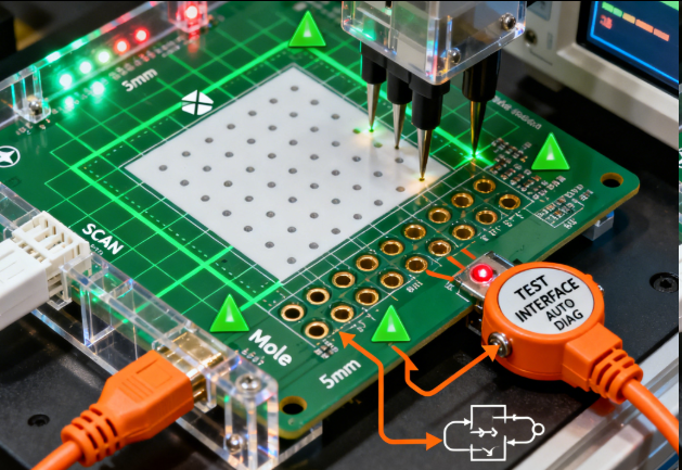
The core of DFT lies in integrating test points and structures that enable comprehensive testing. Key technical considerations include: 1) Test Point Placement: Adding accessible test points (typically 0.8-1.2mm diameter pads) for critical signals—power nets (e.g., +5V, GND), data buses (e.g., I2C, SPI), and component pins (e.g., microcontroller inputs/outputs). Test points should be placed on the top or bottom of the PCB (not between components) and spaced ≥1.2mm apart to accommodate test probes. For high-density PCBs, using “bed-of-nails” test points (arranged in a grid) compatible with automated test fixtures. Ensuring every net has at least one test point—this enables continuity testing (checking for open/short circuits) and signal integrity testing. 2) Boundary Scan (JTAG) Integration: For complex PCBs with high-pin-count components (e.g., FPGAs, microprocessors), implementing the JTAG (Joint Test Action Group) standard (IEEE 1149.1). JTAG uses four dedicated pins (TCK, TMS, TDI, TDO) to access a “boundary scan register” in each JTAG-compliant component, enabling testing of component connections without physical test points. This is critical for BGA (Ball Grid Array) components, where pins are hidden under the package and cannot be probed directly. 3) Built-In Self-Test (BIST): Designing circuits with self-test capabilities—for example, a power management IC with a built-in voltage sensor that verifies output voltage, or a microcontroller that runs a self-test routine on startup to check memory and peripherals. BIST reduces reliance on external test equipment and enables in-field testing (e.g., verifying PCB functionality after installation in a device). 4) Test Fixture Compatibility: Ensuring the PCB design is compatible with test fixtures—adding tooling holes (3-4mm diameter) for aligning the PCB in the fixture, and avoiding components in areas where test probes or fixture clamps will be placed. For panelized PCBs, including test points on the panel (not just individual PCBs) to enable testing of the entire panel before separation.
DFT implementation requires defining test requirements early in the design process—identifying which defects to test for (e.g., short circuits, wrong component values) and selecting appropriate test methods (continuity testing, JTAG, functional testing). Engineers use DFT analysis tools (e.g., Mentor Graphics TestKompress, Cadence DFT Compiler) to verify test point coverage (ensuring ≥95% of nets are testable) and JTAG compliance. Collaboration with test engineering teams is essential to ensure the design meets the capabilities of existing test equipment (e.g., ATE, oscilloscopes).
Application scenarios highlight DFT’s importance. In automotive PCBs (e.g., engine control units), DFT with JTAG enables testing of BGA microcontrollers, detecting hidden solder defects that could cause engine failure. In medical devices (e.g., MRI machine controllers), DFT with BIST ensures every PCB is tested for functional accuracy, complying with regulatory standards (e.g., FDA) and preventing patient harm. In aerospace PCBs (e.g., satellite communication modules), DFT with comprehensive test points enables rigorous testing of signal integrity and power distribution, ensuring reliability in harsh space environments. With manual testing missing up to 30% of defects, DFT is essential for delivering reliable, defect-free PCBs.