-
CN
-
Service Hotline
+8618129931046 Mr. Liao


Time:2025-12-02 Views:1

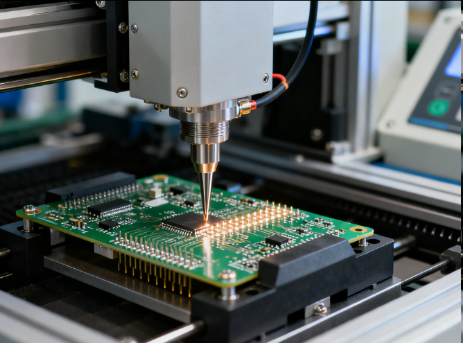
The PCBA (Printed Circuit Board Assembly) test process is a multi-stage procedure designed to ensure electrical functionality, manufacturing quality, and long-term reliability. It begins with pre-test preparation, where assembled boards undergo visual inspection using automated optical inspection (AOI) systems to detect physical defects like solder bridges, missing components, or incorrect polarity. This step reduces downstream testing time by eliminating obvious failures early. The next phase involves in-circuit testing (ICT), which employs needle-bed fixtures to measure component values (e.g., resistors, capacitors) and verify connectivity between nodes. ICT achieves 95–99% fault coverage for open/short circuits and component misplacement, making it critical for high-volume production.
Following ICT, functional testing (FCT) validates the PCBA’s performance under simulated operating conditions. For example, a power supply module might undergo load testing (0–100% output) and dynamic voltage adjustment (±5% tolerance). FCT often integrates environmental stress testing (EST), such as thermal cycling (-40°C to 125°C) or humidity resistance (85% RH for 168 hours), to uncover latent defects. Advanced FCT setups use hardware-in-the-loop (HIL) systems to emulate real-world interfaces (e.g., USB, Ethernet) and validate protocol compliance.
The final stage involves data analysis and feedback. Test results are logged into manufacturing execution systems (MES), which generate quality reports highlighting failure modes (e.g., BGA voiding >25%, capacitor drift beyond ±10%). Root cause analysis (RCA) identifies process weaknesses, such as inconsistent reflow profiles or contaminated solder paste. Continuous improvement loops, driven by AI-powered anomaly detection in oscilloscope data, reduce testing time by 40–60% in automated lines. Compliance with standards like IPC-TM-650 ensures traceability and repeatability across global facilities.