-
CN
-
Service Hotline
+8618129931046 Mr. Liao


Time:2025-05-07 Views:1

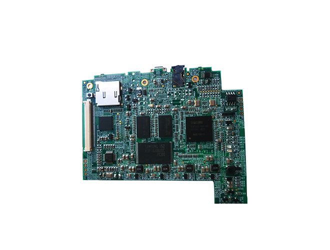
Printed Circuit Board (PCB) routing design for communication equipment is a complex and critical process that directly impacts the performance, reliability, and efficiency of the equipment. Communication devices, such as routers, switches, wireless access points, and base stations, handle high - speed data transmission and require precise PCB routing to ensure signal integrity and minimize interference.
One of the key considerations in PCB routing design for communication equipment is the handling of high - speed signals. These signals, which can operate at frequencies ranging from several gigahertz to tens of gigahertz, are highly sensitive to factors such as trace length, impedance, and crosstalk. To maintain signal integrity, designers use techniques such as controlled - impedance routing, where the impedance of the traces is carefully matched to the source and load impedance. This ensures that the signals are transmitted without reflection, reducing signal loss and distortion. Additionally, differential pairs are commonly used for high - speed data transmission. Differential signaling helps to cancel out common - mode noise and interference, improving the signal - to - noise ratio and the overall performance of the communication equipment.
Another important aspect is the management of power and ground planes. In communication equipment, stable power supply is crucial for the proper operation of high - speed components. The power and ground planes need to be designed with low impedance to minimize voltage drops and power noise. Designers use techniques such as power - plane stitching, where vias are strategically placed to connect different layers of the power plane, reducing the resistance and inductance of the power distribution network. Additionally, proper decoupling capacitors are placed near the power pins of components to filter out high - frequency noise and provide local energy storage, ensuring a stable power supply.
Crosstalk prevention is also a significant challenge in PCB routing design for communication equipment. With multiple high - speed signals being routed on the same PCB, there is a risk of crosstalk, where signals on one trace interfere with signals on adjacent traces. To mitigate crosstalk, designers use techniques such as sufficient trace spacing, shielding, and proper layer - stackup design. Sufficient trace spacing reduces the electromagnetic coupling between traces, while shielding can be used to isolate sensitive traces from interference sources. The layer - stackup design, which determines the arrangement of signal, power, and ground layers, also plays a crucial role in minimizing crosstalk. By carefully considering these factors and implementing appropriate routing techniques, designers can create PCB layouts that enable reliable and high - performance communication equipment.