-
CN
-
Service Hotline
+8618129931046 Mr. Liao


Time:2025-06-18 Views:1

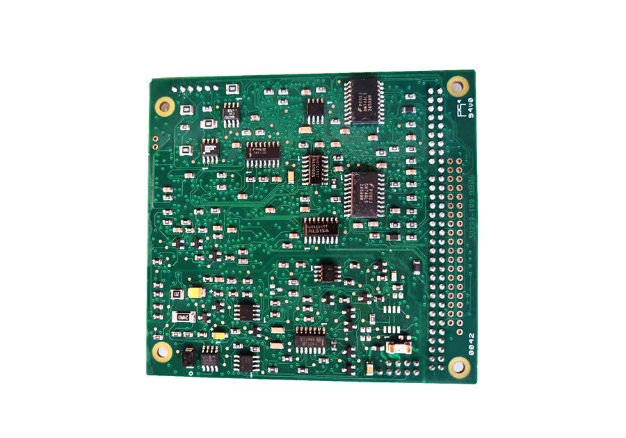
The layout of high-speed connectors on multilayer PCB boards is a complex task that requires careful consideration to ensure optimal signal integrity and reliable performance.
One of the primary considerations is the placement of the connector relative to the components it connects to. High-speed connectors should be positioned as close as possible to the relevant integrated circuits or other devices to minimize the length of the traces. Shorter trace lengths reduce signal attenuation, delay, and the likelihood of signal reflections. For example, when connecting a high-speed USB 3.0 or Thunderbolt connector to a host controller, placing the connector in close proximity to the controller chip can significantly improve the data transfer rate and stability.
Signal routing around the high-speed connector is also critical. Differential pairs, which are commonly used in high-speed interfaces, should be routed symmetrically and with controlled impedance. The traces should be kept away from other high-frequency signals and power traces to avoid crosstalk. Fan-out techniques need to be carefully planned to ensure that the signals can be properly routed from the connector pins to the internal layers of the PCB. Additionally, vias used for signal transition between layers should be optimized in terms of size and placement. Smaller vias with proper anti-pad and thermal relief designs can reduce the parasitic capacitance and inductance, minimizing signal distortion.
Power and ground connections to the high-speed connector are equally important. A stable power supply is required to drive the high-speed signals, and proper grounding helps in reducing EMI and providing a low-impedance return path for the signals. Multiple vias should be used to connect the power and ground planes to the connector pins to reduce the resistance and inductance of the connection. Furthermore, decoupling capacitors should be placed in close proximity to the connector to filter out high-frequency noise and ensure a clean power supply.