-
CN
-
Service Hotline
+8618129931046 Mr. Liao


Time:2025-07-29 Views:1

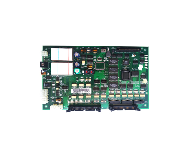
High-frequency filter PCBs are specialized printed circuit boards designed to integrate filtering components for applications operating at radio frequencies (RF), microwave, and beyond. These PCBs play a critical role in reducing electromagnetic interference (EMI) and ensuring signal integrity in high-speed communication systems, such as 5G base stations, radar systems, and satellite transceivers.
The design of high-frequency filter PCBs focuses on minimizing signal loss and maintaining consistent impedance. Substrate materials with low dielectric constant (Dk) and low dissipation factor (Df) are preferred, such as Rogers 4350 or Teflon-based materials, as they reduce signal attenuation at high frequencies. The dielectric constant must be tightly controlled across the board to ensure uniform signal propagation, which is vital for filter performance.
Layout considerations are equally important. Filter components like inductors, capacitors, and resonators are placed strategically to minimize parasitic effects. Short trace lengths between components reduce stray inductance and capacitance, which can degrade filter efficiency. Ground planes are designed as continuous layers to provide a low-impedance return path and shield sensitive components from external interference. Additionally, via placement is optimized to avoid creating unwanted signal paths or disrupting the ground plane.
Manufacturing processes for high-frequency filter PCBs require precision. Controlled impedance routing ensures that signal traces match the characteristic impedance of the system (typically 50 ohms for RF applications), preventing reflections. Plating techniques, such as electroless nickel immersion gold (ENIG), are used to maintain stable electrical connections, even at high frequencies. Testing with network analyzers verifies filter performance, including insertion loss, return loss, and stopband attenuation, ensuring compliance with design specifications.