-
CN
-
Service Hotline
+8618129931046 Mr. Liao


Time:2025-11-05 Views:1

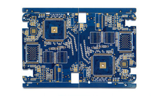
High-Density PCBA (Printed Circuit Board Assembly) Design refers to the creation of PCBs with minimized component spacing, reduced trace widths, and increased component density—enabling smaller form factors while supporting complex functionality. This design approach is critical for modern electronics like smartphones, wearables, IoT sensors, and medical devices, where space constraints demand packing more components (e.g., microchips, passives, and connectors) into compact areas.
The core of high-density design lies in optimizing three key elements: component selection, trace routing, and layer utilization. First, component selection prioritizes miniaturized packages: 01005 (0.4mm×0.2mm) passives, wafer-level chip-scale packages (WLCSP), and ball grid arrays (BGA) with fine pitch (≤0.5mm) are common. These components reduce footprint size by 50–70% compared to traditional packages, but require precise placement and soldering. For example, a WLCSP with 0.3mm pitch has solder balls spaced just 0.3mm apart, demanding 严格 control over solder paste volume to avoid short circuits.
Second, trace routing uses narrow trace widths (often 0.1–0.2mm) and minimal spacing (0.1mm or less) to fit more traces on the board. Designers rely on CAD tools like Altium Designer or Cadence Allegro to implement differential pair routing—critical for high-speed signals (e.g., USB 3.2, PCIe 5.0) to minimize crosstalk. Ground planes are strategically placed beneath signal traces to reduce electromagnetic interference (EMI), and vias (especially microvias with ≤0.15mm diameter) are used to connect traces across layers without occupying surface space.
Third, layer utilization maximizes vertical space through multi-layer designs (often 6–12 layers for high-density PCBs). Inner layers are dedicated to power distribution or ground planes, while outer layers hold components. Blind and buried vias (which only connect specific layers) eliminate the need for through-holes that would otherwise block surface space.
High-density design also requires addressing unique challenges: thermal management (closely packed components generate more heat, requiring heat sinks or thermal vias), manufacturability (designs must comply with IPC-2221 standards to ensure compatibility with SMT assembly), and testability (test points may be omitted due to space, requiring boundary scan testing or X-ray inspection).
This design approach enables innovations like ultra-thin smartphones (with PCBs occupying <10% of internal space) and wearable health monitors (small enough to fit on a wrist). However, it demands collaboration between designers and manufacturers to balance density with reliability—even minor design flaws (e.g., insufficient trace spacing) can render the PCB unmanufacturable.