-
CN
-
Service Hotline
+8618129931046 Mr. Liao


Time:2025-07-08 Views:1

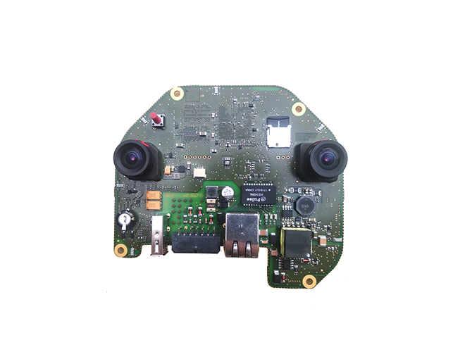
Printed Circuit Boards (PCBs) are integral to modern electronics, and their failure can lead to significant system malfunctions. The failure analysis of PCBs involves a systematic approach to identify the root cause of issues. The first step is visual inspection, which uses microscopes and imaging techniques to detect visible defects like cracks, shorts, or component damage. For instance, a magnified view can reveal tiny cracks in solder joints that may cause intermittent electrical connections.
Next, electrical testing plays a crucial role. Tools such as circuit testers and analyzers are employed to measure electrical parameters, identify open circuits, short circuits, and impedance mismatches. In some cases, time-domain reflectometry (TDR) is used to detect discontinuities in transmission lines, helping to pinpoint faulty sections of the PCB.
Failure analysis also includes material characterization. Techniques like X-ray diffraction (XRD) and scanning electron microscopy (SEM) are utilized to examine the physical and chemical properties of PCB materials. XRD can analyze the crystal structure of metals, while SEM provides high-resolution images of the surface, enabling the identification of corrosion, oxidation, or material degradation.
Moreover, thermal analysis methods, such as infrared thermography, are used to detect abnormal heat generation, which may indicate overloading or poor thermal management. By combining these multiple analysis methods, engineers can accurately diagnose PCB failures, develop corrective measures, and enhance the reliability and lifespan of electronic products.