-
CN
-
Service Hotline
+8618129931046 Mr. Liao


Time:2025-07-16 Views:1

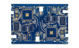
Buried vias in double - sided printed circuit boards (PCBs) offer significant advantages in terms of circuit density and signal integrity, but their design requires careful consideration and specific techniques to ensure optimal performance. Buried vias are connections that are hidden within the layers of the PCB, not extending to the outer surfaces, which helps in reducing the overall footprint and improving the routing flexibility.
One of the primary design techniques is proper via placement planning. When designing a double - sided board with buried vias, engineers need to analyze the circuit layout thoroughly. They should identify the critical signal paths and component locations first. For high - speed signals, buried vias should be placed strategically to minimize the length of the trace segments and reduce signal reflections. By keeping the via - to - via and via - to - component distances as short as possible, the inductance and capacitance associated with the vias can be minimized, improving the signal integrity. For example, in a high - frequency communication circuit, vias for differential pairs should be placed symmetrically to maintain the balanced nature of the signals.
Another important aspect is the selection of via dimensions. The diameter of the buried via, including the drill size and the annular ring, needs to be optimized. A smaller drill size can save more space on the PCB, but it also increases the resistance and inductance of the via. On the other hand, a larger drill size may be easier to manufacture but could limit the routing density. Typically, the drill size for buried vias in double - sided boards ranges from 0.2 - 0.4 mm, and the annular ring width should be at least 0.1 mm to ensure reliable electrical connection and mechanical strength. Additionally, the aspect ratio (the ratio of the drill depth to the drill diameter) should be considered. A high aspect ratio can pose challenges during the drilling process and may lead to issues such as drill breakage or poor plating quality.
The design of the pads around the buried vias also matters. Thermal relief pads can be used to improve the heat dissipation during the soldering process and prevent excessive heat accumulation, which could damage the PCB or the components. For power - related vias, larger pads or multiple vias in parallel can be employed to handle higher currents. Moreover, the isolation between adjacent vias and traces should be carefully maintained to avoid crosstalk. Adequate clearance rules need to be set in the PCB design software to ensure that the electromagnetic fields of different signal paths do not interfere with each other. By mastering these design techniques, engineers can effectively utilize buried vias in double - sided boards to create more compact, reliable, and high - performance circuit designs.