-
CN
-
Service Hotline
+8618129931046 Mr. Liao


Time:2025-10-24 Views:1

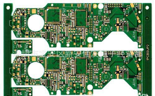
Wearable device PCB circuit boards are specialized printed circuit boards that are meticulously designed to meet the unique and stringent requirements of wearable electronics, which have become an indispensable part of modern life, encompassing a wide range of products from fitness trackers and smartwatches to health - monitoring devices and augmented - reality glasses. These PCB boards must balance multiple critical factors, including size, weight, power consumption, functionality, and reliability, to enable the seamless integration of various components into compact, lightweight, and comfortable wearable form factors.
Size and weight are of utmost importance in the design of wearable device PCB circuit boards. Since these devices are intended to be worn on the body for extended periods, the PCB boards need to be as small and lightweight as possible without compromising on functionality. To achieve this, advanced PCB manufacturing techniques are employed. High - density interconnect (HDI) technology is widely used, which allows for the creation of smaller trace widths, smaller vias, and multiple layers. This enables a large number of components, including microcontrollers, sensors, wireless communication modules, and power - management circuits, to be integrated into a limited space. Surface - mount technology (SMT) is also extensively utilized, as it allows for the placement of small - sized components on both the top and bottom surfaces of the PCB, further maximizing component density. Additionally, 3D - stacking and system - in - package (SiP) technologies are increasingly being adopted to reduce the overall footprint and thickness of the PCB, making the wearable devices more compact and comfortable to wear.
Power consumption is another critical aspect that wearable device PCB circuit boards must address. Most wearable devices are battery - powered, and optimizing power usage is essential to extend the battery life and enhance the user experience. The PCB boards are designed with highly efficient power - management circuits. These circuits include voltage - regulation modules that convert the input power from the battery into stable and appropriate voltage levels for different components on the board. Power - saving features, such as dynamic voltage and frequency scaling (DVFS), sleep - mode control, and power - gating, are integrated to minimize power consumption when components are not in active use. For example, in a smartwatch, the display and some sensors can be put into a low - power sleep mode when the device is not in use, reducing power consumption significantly. Moreover, the selection of low - power components, such as low - power microcontrollers, sensors, and wireless communication modules, also plays a crucial role in reducing the overall power consumption of the wearable device.
Functionality is a key consideration in the design of wearable device PCB circuit boards. These boards need to support a wide range of functions, including sensing, data processing, wireless communication, and user - interface control. A variety of sensors, such as accelerometers, gyroscopes, heart - rate monitors, and temperature sensors, are integrated onto the PCB to enable functions like activity tracking, health monitoring, and motion sensing. High - performance microcontrollers or application - specific integrated circuits (ASICs) are used for data processing, running complex algorithms to analyze the sensor data and perform various functions. Wireless communication modules, such as Bluetooth, Wi - Fi, or cellular modules, are incorporated to enable seamless data transfer between the wearable device and other devices, such as smartphones or cloud - based servers. User - interface components, such as touchscreens, buttons, and haptic feedback devices, are also connected to the PCB to provide an intuitive and interactive user experience.
Reliability is non - negotiable for wearable device PCB circuit boards. These devices are exposed to various environmental conditions, including moisture, temperature changes, and mechanical stress. To ensure reliability, the PCB boards are designed with robust materials and manufacturing processes. Surface finishes, such as immersion gold or electroless nickel immersion gold (ENIG), are used to improve the corrosion resistance and solderability of the PCB. The components are mounted on the board using high - quality soldering techniques to ensure strong and reliable connections. Additionally, the PCB boards are often encapsulated or potted with protective materials to provide additional protection against moisture, dust, and mechanical shock. By carefully considering and optimizing these aspects, wearable device PCB circuit boards can meet the demanding requirements of modern wearable electronics, providing users with reliable, functional, and comfortable wearable devices.